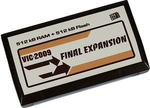
|
Pin |
Name
|
Description |
Pin |
Name
|
Description |
|
1 |
GND |
System ground |
A |
GND |
System ground |
|
2 |
CD0 |
Data bus bit 0 |
B |
CA0 |
Address bus bit 0 |
|
3 |
CD1 |
Data bus bit 1 |
C |
CA1 |
Address bus bit 1 |
|
4 |
CD2 |
Data bus bit 2 |
D |
CA2 |
Address bus bit 2 |
|
5 |
CD3 |
Data bus bit 3 |
E |
CA3 |
Address bus bit 3 |
|
6 |
CD4 |
Data bus bit 4 |
F |
CA4 |
Address bus bit 4 |
|
7 |
CD5 |
Data bus bit 5 |
H |
CA5 |
Address bus bit 5 |
|
8 |
CD6 |
Data bus bit 6 |
J |
CA6 |
Address bus bit 6 |
|
9 |
CD7 |
Data bus bit 7 |
K |
CA7 |
Address bus bit 7 |
|
10 |
/BLK1 |
8K decoded RAM/ROM block 1 ($2000 - $3FFF) |
L |
CA8 |
Address bus bit 8 |
|
11 |
/BLK2 |
8K decoded RAM/ROM block 2 ($4000 - $5FFF) |
M |
CA9 |
Address bus bit 9 |
|
12 |
/BLK3 |
8K decoded RAM/ROM block 3 ($6000 - $7FFF) |
N |
CA10 |
Address bus bit 10 |
|
13 |
/BLK5 |
8K decoded RAM/ROM block 5 ($A000 - $BFFF) |
P |
CA11 |
Address bus bit 11 |
|
14 |
/RAM1 |
1K decoded RAM block ($0400 - $07FF) |
R |
CA12 |
Address bus bit 12 |
|
15 |
/RAM2 |
1K decoded RAM block ($0800 - $0BFF) |
S |
CA13 |
Address bus bit 13 |
|
16 |
/RAM3 |
1K decoded RAM block ($0C00 - $0FFF) |
T |
/I/O2 |
I/O block 2 (located at $9600) |
|
17 |
VR/W |
Read/Write line from VIC chip (high-read, low-write) |
U |
/I/O3 |
I/O block 3 (located at $9C00) |
|
18 |
CR/W |
Read/Write line from CPU (high-read, low-write) |
V |
S02 |
Phase 2 System Clock |
|
19 |
/IRQ |
Interrupt request line to 6502 |
W |
/NMI |
6502 Non maskable interrupt |
|
20 |
n/c |
Not connected |
X |
/RESET |
6502 Reset pin |
|
21 |
+5V |
+5 VDC |
Y |
n/c |
Not connected |
|
22 |
GND |
System ground |
Z |
GND |
System ground |
 Tarpeellista
tavaraa VIC-20 -konetta varten.


